Semiconductor
Elastomer seals for semiconductor production face incredibly challenging environments – including aggressive plasma chemistries, and extreme temperatures.
PPE material grades have been engineered to offer enhanced performance with reduced particle generation, to minimize yield loss.
We manufacture bespoke components for:

Semiconductor integrated circuits

Flat panel displays (FPD)

Solar cells (crystalline, multi-crystalline, concentrator)

MEMS

LED / OLED

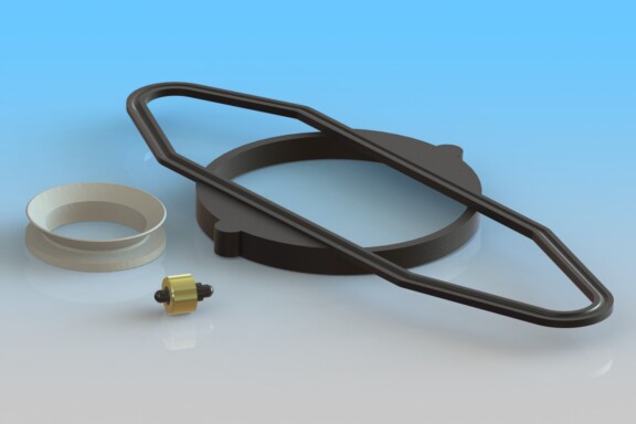
Semiconductor sealing solutions
PPE provides clean room manufactured seals with low particle and low trace metal contamination for minimized yield loss and low chemical erosion rates that offer the following benefits:
Extended system up-time
Increased mean time between failure (MTBF)
Decreased wet or mechanical clean frequency
Minimized cost of ownership (CoO)
Extended system up-time expand_more
Increased mean time between failure (MTBF) expand_more
Decreased wet or mechanical clean frequency expand_more
Minimized cost of ownership (CoO) expand_more
Semiconductor manufacturing processes
Find out more about thermal, plasma and wet chemical processes, and how PPE’s range of elastomer seals for semiconductor applications like these can represent a significant operational advantage.
Plasma Processes
Thermal Processes
Wet Chemical Processes
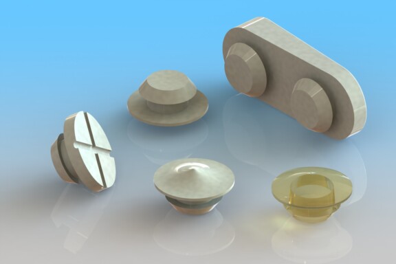
Products for semiconductor applications
Take a look at some of the key sealing products we supply to the semiconductor industry.
Semiconductor O-rings
Custom Seals
Wafer Handling Components
KF-ISO-NW Flange Fittings
Micro Seals
Slit Valve Doors
Need more help? Speak to one of our experts today.
Looking for more technical detail? Check out our Resources & Tools.
Resources
Browse our key resources on elastomer sealing for semiconductor applications, including videos, animations, brochures and webinars.
For our full range of support material, visit our Resources page.


