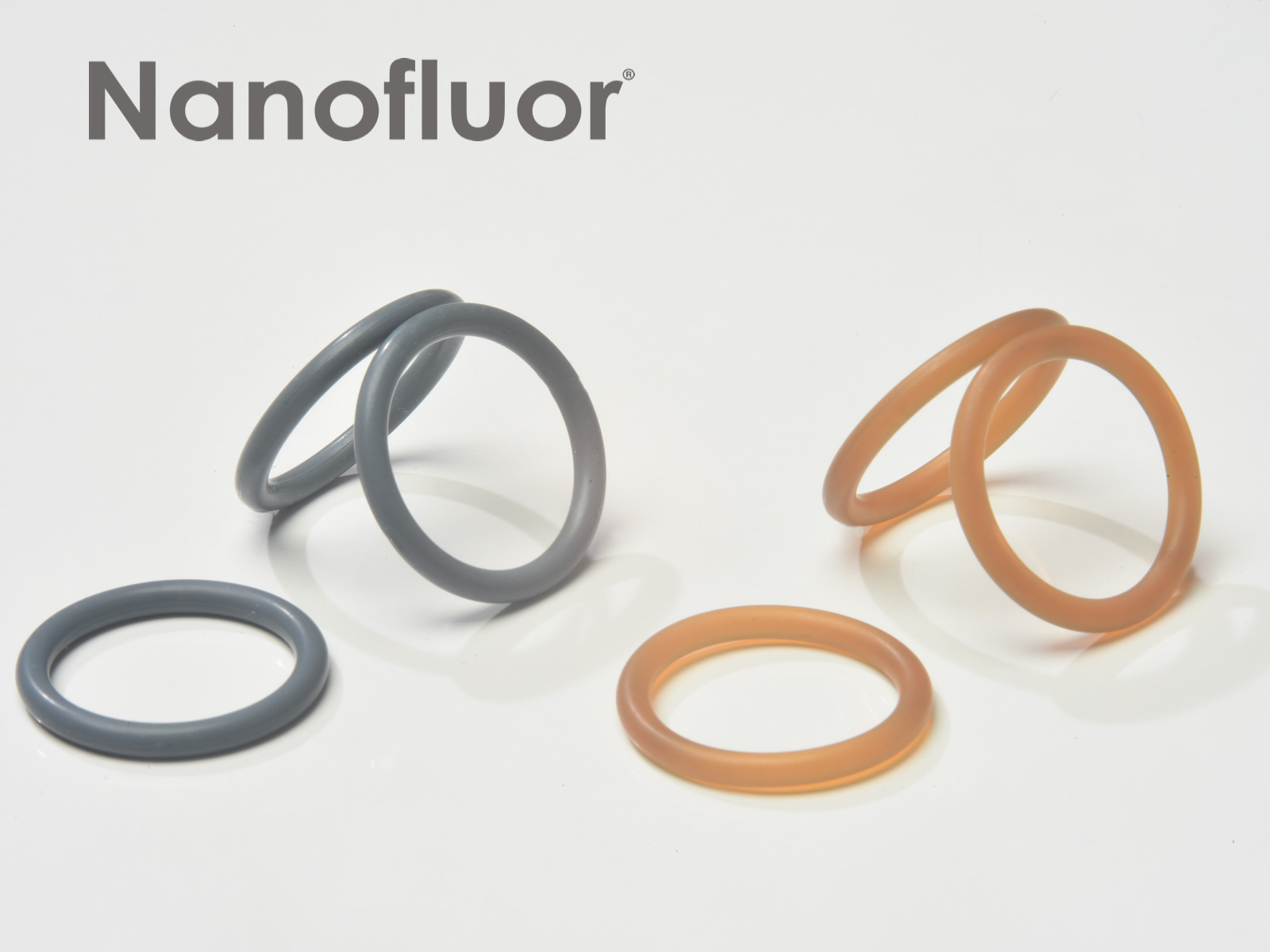
+44 (0)1254 295400

Nano-filled Materials

The highly plasma resistant nano-filled materials provide a unique and process optimized sealing solution for many semiconductor process applications.

Available as O-rings and other seal shapes, the nano-filled materials are designed for use in critical applications, where the seal is in direct contact with the chemistry:

  • All tool locations in contact with plasma
  • Chamber lid seal
  • Chamber window seals
  • Plasma source
  • Critical component protection 

The uniquely compounded materials ensure low plasma erosion rates and increased seal lifetime, and coupled with low trace metal content, the risk of lowered yield and warranty failures are reduced.

Nano-filled materials:

Nanofluor® Y75G is a highly fluorinated elastomer which incorporates relatively low levels of an advanced nanoparticle type filler system, producing a clean compound formulated for minimum particle generation, combined with excellent resistance to aggressive oxygen and fluorine based plasmas. The material has been formulated to be used in critical locations where the seal can be directly exposed to the chemical environment.

Perlast® G67G is a perfluoroelastomer which incorporates low levels of an advanced nano-particle type filler system. It is a clean compound formulated for minimum particle generation, combined with excellent resistance to aggressive oxygen, chlorine and fluorine based plasmas. The material has been formulated to be used in critical locations where the seal can be directly exposed to the chemical environment.

Both nano-filled materials are formulated with low levels of nano-particle filler and the achievement of low filler particle agglomeration, resulting in minimized risk of particle generation or large particle contamination.

SEM Image Nano-filled materials

These materials are specifically developed to resist harsh plasma conditions that perform significantly better than any other sealing materials.

Benefits:

  • High purity inorganic filler
  • 35nm average particle size
  • Highest level of plasma resistance
  • High purity base polymer
  • Low risk of yield reduction
  • Maintain device electrical characteristics
  • Low cost of consumables
  • Low concentration nano-particle filler system
  • Low agglomeration compound


Weight Loss Upon Plasma Exposure Graph

Sourcing an appropriate sealing material is critical to avoid wafer contamination which can reduce yield. In addition to this, it is also important to ensure seal lifetime compatibility with existing maintenance cycles and potentially facilitate an increase to the process tool productive period or uptime leading to lower cost of consumables.

Precision Polymer Engineering is not just a provider of seal materials, but customised engineered solutions for critical sealing applications, in order to maximise seal integrity and longevity thereby reducing cost of consumables and increasing the potential to retain aftermarket sales.

How can we help? Contact us to discuss your semiconductor sealing requirements.

Send us your requirements

Let us know what you need and we'll respond with out best offer.

, we've completed some of this form to save you time. Not you? Click here.

* Don’t worry we won’t spam you and you can unsubscribe at any time.

People also viewed...

Join our mailing list to receive the quarterly PPE enewsletter and be the first to know about all the latest news
Thanks for joining our enewsletter mailing list.

We'll need some basic details first

Please provide a valid email address to access the datasheet

* Don’t worry we won’t spam you and you can unsubscribe at any time.